
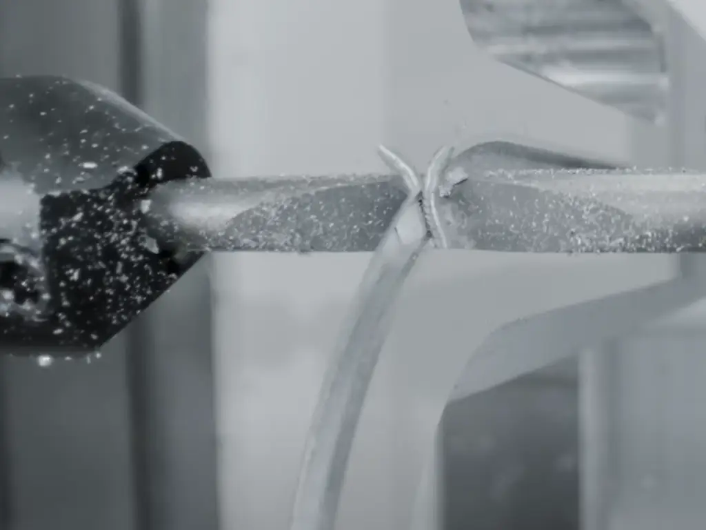
The semiconductor manufacturing industry is a world where everything is done at a microscopic level and precision is the norm. One errant particle or a small dimensional error can ruin a whole production run. The industry runs on a system of extremely advanced machinery, and at the core of that machinery are precision parts that are machined to an extremely high degree of high accuracy.
This is the field of semiconductor CNC machining. It is not just a step up in sophistication from conventional machining; it is a specialized field that combines high precision, contamination control, and material science. This paper gives a detailed description of this technical area. We will examine the fundamental needs that characterize it, the high-tech materials that make it possible, and the essential applications that rely on it, providing an authoritative guide to engineers, procurement managers, and industry innovators from leading semiconductor manufacturers.
Why Standard CNC Machining Falls Short for the Semiconductor Industry
In order to appreciate the special needs of CNCprecision machining to the semiconductor industry, it is worth noting why traditional machining techniques are inadequate. Although a typical machine shop is capable of making high-quality parts with tolerances that are appropriate for an industry such as automotive or general manufacturing, the semiconductor industry requires a much greater degree of precision and control. This is because there are three significant challenges that are beyond the scope of conventional CNC machining.
- To begin with, semiconductor production is on a scale that is drastically smaller.Photolithography and other processes need nanometer accuracy and the machines used must handle silicon wafers with micrometer (um) precision. Even the slightest dimensional inaccuracies in parts like wafer handlers or vacuum chamber seals can lead to wafer damage, which stops production and leads to significant financial losses.
- Second, it is important to control contamination. Small particles or fluid residues are not a problem in a typical machining setting. But in semiconductor manufacturing, even minute contaminants, such as a metallic flake or organic film, can ruin an entire chip or batch. Thus, machining operations should follow stringent cleanroom guidelines to guarantee that parts are within the zero-contamination requirements of the industry, safeguarding delicate electronics like smartphones and IoT devices.
Lastly, semiconductor equipment should be able to endure harsh operating conditions. Components are frequently exposed to high vacuum conditions, corrosive gases, aggressive plasmas, and large temperature variations. Under these stresses, materials that are acceptable in typical industrial environments can deform, corrode, or emit contaminants, and are not acceptable in semiconductor applications. These are severe requirements that need high-level CNC machining that is way above the norm.
The Core Pillars of Semiconductor CNC Machining

In order to satisfy these unprecedented requirements, the art of semiconductor CNC machining is anchored on three pillars. Any supplier in this area must be competent in all three to achieve excellence.
- Uncompromising Precision & Ultra-Tight Tolerances: The most important requirement is precision. This includes machining to tight tolerances that are frequently quoted in single-digit microns (e.g. +/- 0.005 mm). This is only possible with a full system, beginning with state-of-the-art multi-axis modern CNC machines, especially 5-axis centers. Such a CNC machine is able to create complex geometries in one set up, reducing the tolerance stacking errors that may be introduced by moving and re-fixturing a workpiece on the chuck. This level of automation also requires a temperature-controlled environment and sophisticated metrology equipment, such as Coordinate Measuring Machines (CMMs), to check all dimensions and ensure perfect consistency.
- Absolute Purity & Contamination Control: Where the form of the part is characterized by precision, the surface integrity is characterized by purity. This pillar demands that the components are machined, handled, cleaned, and packaged without introducing any foreign material. This implies processing components in a certified cleanroom (usually ISO 5 / Class 100), with special cleaning processes, and final packaging in secure, anti-static packaging. The aim is to provide a component that will not add contaminants to the cleanroom environment in which it will be deployed, maintaining a low surface roughness (Ra).
- Mastery of Advanced Engineering Materials: The third pillar is a profound, practical material knowledge. Semiconductor equipment materials are chosen based on their performance properties in harsh conditions. The machining of these hard materials is science. A machinist using a CNC milling machine must know how every polymer or alloy will react to the cutting tool and its spindleRPM to obtain the desired shape and surface finish without damaging the structural integrity of the material. This deep understanding builds upon the fundamentals of what is cnc milling and its core principles. This versatility in handling different materials is key.
These three pillars,precision, purity, and mastery of materials, are the pillars on which all successful semiconductor CNC machining operations must be built. It is not a single strength that makes excellence in this field, but a combination of the three. It is only through the complete adoption of this triad that manufacturers can satisfy the uncompromising demands of the industry in terms of accuracy, cleanliness, and performance of each component supplied.
Choosing the Right Material for Semiconductor CNC Machining
The choice of material is a critical decision that directly impacts a component’s performance, lifespan, and effect on the manufacturing process. The selection is a balance of properties like chemical resistance, thermal stability, and mechanical strength, all of which influence final production costs.
High-Performance Engineering Plastics
Polymers are important where electrical insulation or direct, non-destructive contact with wafers is needed. Materials like polycarbonate and POM are also common in less critical applications.
| Material | Key Properties | Typical Applications |
| Polyimide (PI) | Excellent thermal stability, low outgassing | Wafer clamps, test sockets, lift pins |
| PEEK | High mechanical and chemical resistance | Vacuum wands, insulators, structural parts |
| PTFE | Exceptional chemical inertness | Seals, gaskets, valve parts |
| PAI | High strength and stiffness at elevated temperatures | High-load components, test sockets |
| PBI | Highest heat resistance and lowest outgassing among unfilled plastics | Extreme vacuum and high-temperature environments |
High-tech Ceramics
Technical ceramics are used where extreme hardness, thermal stability, and resistance to plasma erosion are needed. They are difficult to machine, sometimes requiring Electrical Discharge Machining (EDM), but their performance is unmatched.
| Material | Key Properties | Typical Applications |
| Alumina (Al₂O₃) | High hardness, good electrical insulation and thermal conductivity | Insulators, chamber parts, end effectors |
| Silicon Carbide (SiC) | Exceptional hardness, thermal conductivity, and plasma resistance | Plasma etch chamber parts (e.g., showerheads, chucks) |
Specialized Metals and Alloys
Metals and composites are needed because of their strength, stiffness, and conductivity, especially in structural and vacuum applications.
| Material | Key Properties | Typical Applications |
| Stainless Steel (316L) | Corrosion resistant, standard for vacuum systems | Vacuum chambers, flanges, gas delivery components |
| Aluminum (6061) | Lightweight, excellent machinability and thermal conductivity | Chamber bodies, heat sinks |
| Titanium | High strength-to-weight ratio | Robotic components, aerospace applications |
| Copper (OFE) | High purity, excellent thermal and electrical conductivity | Heat sinks, sputtering targets |
| Low-Expansion Alloys (FeNi36) | Very low thermal expansion | Optical mounts, precision instruments |
Conclusion
Choosing the appropriate material is not just a matter of matching properties, it is a matter of matching properties to the purpose, the environment and the performance requirements of each part. As semiconductor systems become more complex, material selection is an innovation and reliability driver.
Common Applications & Components Made by CNC Machining
To bring these concepts more to life, consider the physical parts that rely on this level of production, which usually includes bothCNC milling and CNC turning processes.
- Wafer Handling End Effectors: Robotic components that transfer wafers, which have to be flawlessly flat and non-contaminating.
- Vacuum Chambers: The sealed areas of processes like deposition and etching, which must have airtight integrity.
- Gas Delivery Manifolds: Complicated components with intricate internal channels to precisely mix and distribute process gases.
- Wafer Chucks (Pedestals): Stands that hold wafers, usually electrostatically, which are machined on a lathe or mill and must be very flat so that they can be processed evenly.
- Test Sockets and Probe Cards: Components used in final testing, and which must be extremely dimensionally precise to mate thousands of microscopic contacts, and are often regarded as a type of specialized tooling.
What to Demand From Your Machining Partner
In outsourcing key parts, whether the supplier is local or abroad, it is not sufficient to know the technical specifications. What is more important is that you should make sure that your supplier is able to meet those requirements on a regular basis. A reliable partner must be capable of giving clear and dependable evidence of their abilities, and not mere words.
An excellent machining partner must possess a certified quality system like ISO 9001. This certification ensures that there is uniformity in production and that thousands of the same parts can be produced. It also implies that they are able to offer complete material traceability, which clearly indicates the origin and specifications of each stock item. All major processes, including CAD/CAM programming and final inspection, must be documented and repeatable. This degree of documentation is the basis of a reliable supply chain.
The finest suppliers will even become part of your engineering team. They provide Design for Manufacturability (DFM) comments– an expert analysis of your design and recommendations that can enhance quality, reduce cost, or shorten lead times, without affecting the functionality of the part. An active partner in this process is showing a sincere interest in the success of your project.
Your Strategic Partner: How We Deliver Value in Semiconductor CNC Machining

At U-Need, our roots run deep in precision machining — with over 30 years of collective experience, our engineering team (averaging 15+ years per engineer) understands the uncompromising demands of the semiconductor industry. We’ve successfully served 300+ clients across 20+ countries, delivering more than 35,000 custom non-standard parts. Our strength lies in micro-tolerance capabilities — achieving up to ±0.001mm — and in mastering complex geometries like 0.02mm inner and outer corner radii, ideal for semiconductor molds and components.
Integrated, High-End Manufacturing Ecosystem Our production line is built for semiconductor excellence. Equipped with industry-leading machines like Japan’s Takisawa CNC lathes, Swiss GF AgieCharmilles wire EDMs, and PG optical curve grinders, we provide full-process machining — from turning, milling, and grinding to EDM and stamping. We also offer advanced specialty techniques such as mirror EDM and PG grinding for ultra-flat surfaces and tight-tolerance parts, often required in semiconductor tooling. These capabilities allow us to deliver samples in as fast as 3–5 days, ensuring your time-to-market stays competitive.
Custom-Centric Engineering and Quality Commitment We treat every project as a precision challenge — not just a job. Whether you’re prototyping a single component or scaling a complex assembly, we support full customization of materials (metal, plastic, ceramic), dimensions, and finishes with no MOQ restrictions. Backed byISO 9001:2015 certification and a 99.3% pass rate, our rigorous QC process spans raw material inspection to full-dimensional final checks. Plus, with 24-hour quote turnaround and 1-year warranty support, we stay responsive and accountable at every stage of your product lifecycle.
The Future of Semiconductor Manufacturing and the Role of CNC Machining

The semiconductor industry continues to evolve rapidly. New technologies like EUV photolithography and advanced chiplet packaging are pushing the boundaries of manufacturing. These advancements place even greater demands on the underlying equipment and its components.
The future will require components with even more complex geometries and tighter tolerances. The role of the expert precisionCNCmachining partner will become even more critical, evolving from a simple make-to-print service to a collaborative relationship where deep machining expertise and knowledge of numerical control informs the design of next-generation tools from the beginning.
In conclusion, semiconductor CNC machining is a field where precision, purity, and material science are paramount. Success is the result of deliberate investment, deep expertise, and an unwavering commitment to quality systems. Choosing a manufacturing partner is a critical decision that requires finding a team that not only possesses the right equipment but also proves their commitment through certified processes and a collaborative spirit. If you are seeking a partner ready to meet the challenges of today and tomorrow, we are ready to build with you.

 English
  German
  French
  Italian
  Spanish
  Polish
  Czech
Czech  Japanese